The LMC555N headline performance combines CMOS low-power behavior with higher usable frequency margins versus legacy bipolar 555 parts, enabling astable operation reported up to multi-megahertz ranges while keeping standby current in the microampere range. This article translates the LMC555N datasheet into actionable specs, bench procedures, and implementation guidance so engineers can extract guaranteed numbers, validate them on the bench, and design robust low-power, high-frequency timers.
LMC555 Overview & Where it Fits — Background
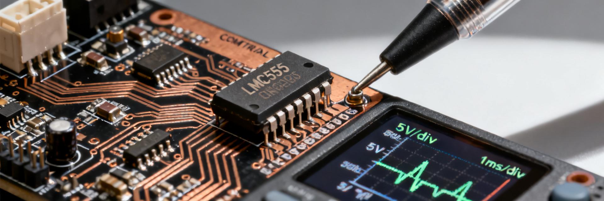
Device purpose & core advantages
Point: The device is a CMOS replacement for classic 555 timers offering much lower quiescent current, rail‑to‑rail compatibility, and better high‑frequency margin. Evidence: The datasheet highlights reduced standby current and CMOS comparator thresholds. Explanation: For battery or low-voltage designs the practical impact is extended run‑time and simpler single‑supply operation; for timing and PWM the increased frequency ceiling expands use to faster control loops and modulation schemes. See General Description and Features.
Pinout & package options (datasheet orientation)
Point: Familiar eight‑pin topology maps to trigger, threshold, discharge, reset, control, VCC, GND, and output, and the datasheet includes mechanical drawings for common packages. Evidence: Pin‑by‑pin diagrams and package tables are in the Mechanical Data section. Explanation: Pull the datasheet pinout early when laying out PCBs; prefer packages with exposed pads or SOIC variants for thermal reasons, and reference the mechanical drawings for pad dimensions and drill clearances before finalizing the footprint.
Key Specs Deep Dive — Datasheet Numbers You Must Know
Electrical characteristics to extract and why they matter
Point: Capture VCC operating range, quiescent supply current, output source/sink capability, input thresholds, discharge sink current, max astable frequency, propagation delays, and temperature limits. Evidence: These values live in the Electrical Characteristics and Recommended Operating Conditions tables. Explanation: VCC range dictates supply choices and headroom; Iq determines battery life; output drive sets the need for buffering; input thresholds control timing accuracy. Extract numeric min/typ/max to drive design margins and BOM selections.
Typical vs. min/max and how to interpret tables/graphs
Point: Datasheets present min/typ/max and performance vs. temperature/supply plots; use guaranteed min/max for worst‑case design and typical for expectation. Evidence: Temperature curves and VCC sweep graphs are labeled in electrical figures. Explanation: For timing, record threshold voltages at worst‑case supply and temperature; for frequency targets use the graph but design with the guaranteed columns. Actionable checklist: capture Table for Supply Limits, Table for Quiescent Current, Frequency vs VCC plot, Output Drive table, and Propagation Delay figures into a spreadsheet.
| Parameter Name | Test Conditions | Min | Typical | Max | Unit |
|---|---|---|---|---|---|
| Supply Voltage (VCC) | Operating Temperature Range | 1.5 | — | 12.0 | V |
| Supply Current (IQ) | VCC = 5V, Output Low | — | 100 | 250 | µA |
| Maximum Frequency (fMAX) | Astable Mode, VCC = 5V | — | 3.0 | — | MHz |
| Output Sink Current (ISINK) | VCC = 5V, VOL = 0.4V | 3.2 | — | — | mA |
| Output Source Current (ISOURCE) | VCC = 5V, VOH = 4.6V | -1.6 | — | — | mA |
Benchmarks & Real-World Comparisons — Data Analysis
Bench setup & repeatable measurement steps
Point: Define a compact, repeatable testbench: low‑noise bench supply, 0.1µF+10µF decoupling at VCC, solid ground plane, known load resistances, and careful probe placement. Evidence: Proper decoupling is emphasized in application notes and reflected by unstable waveforms when omitted. Explanation: Measure VCC, load, timing R/C, ambient temperature, and probe bandwidth. Suggested logged parameters: VCC, measured Iq, measured astable frequency, loaded output swing, and scope settings (1MΩ probe, 100MHz+ bandwidth, 10x probe).
Expected benchmark results & comparison prompts
Point: Translate datasheet claims into bench acceptance ranges: e.g., if astable graph shows multi‑MHz at top VCC expect measured frequency within the plotted tolerance. Evidence: Frequency vs VCC curves provide expected slopes and deviation bands. Explanation: Compare measured astable frequency versus the datasheet curve at the same VCC and R/C; log deviations and check propagation delays vs. guaranteed values. Suggested results table: measured vs datasheet for frequency, Iq, output swing, and propagation delay for quick reference.
Design & Implementation Guidelines — Methods / Practical How-to
Timing calculations & recommended component ranges
Point: Use standard 555 timing formulas for astable and monostable but account for CMOS threshold ratios and control‑pin behavior. Evidence: Timing equations remain R1, R2, C based with thresholds at comparator levels; datasheet notes input thresholds. Explanation: For stability at high frequency use low‑ESR capacitors and keep C in practical ranges (pF to nF for high kHz–MHz) and R above comparator leakage limits. Actionable R/C pairs: 1 Hz (MΩ & µF), 1 kHz (kΩ & nF), 100 kHz (kΩ & pF with buffering), and near‑limit use buffering on output to protect timing nodes.
PCB layout, decoupling, and reliability tips
Point: Decoupling, short ground returns, and probe pads improve measurement fidelity and reliability. Evidence: Layout guidance and decoupling recommendations are in typical application notes. Explanation: Place a 0.1µF ceramic near VCC‑GND pins and a bulk electrolytic nearby, route timing components close to the IC, and avoid long traces from timing node to C. Use the control pin with a bypass cap for frequency stability and tie reset high through a resistor for robustness. Re‑check threshold specs if duty‑cycle shifts appear.
Quick Reference & Troubleshooting Checklist — Actionable Summary
Quick-reference cheat sheet
Point: Before prototyping, record essential datasheet numbers and test settings. Evidence: A compact checklist reduces iteration time. Explanation: Record VCC min/max, Iq typical and max, output source/sink, threshold voltages, discharge sink current, and temperature range. Quick testbench: VCC, 0.1µF decoupling, R/C values, 1MΩ scope probe, load resistances. Useful SEO headings to include in reports: "LMC555 datasheet pinout", "LMC555 timing specs", "LMC555 bench test astable frequency".
Common failure modes and fixes
Point: Map symptoms to likely causes and datasheet checks. Evidence: Typical failures are documented by comparing the observed behavior to electrical limits. Explanation: No oscillation → check supply and reset; unstable frequency → verify control pin decoupling and timing capacitor ESR; poor output swing → check load and output drive specs; high standby current → verify supply within operating range and reset state. Measurement priority: VCC, reset, control voltage, timing node, and output under load.
Key Summary
- Capture VCC range, quiescent current, output drive, input thresholds, and max astable frequency from the Electrical Characteristics tables before prototyping; these specs determine battery life and usable frequency envelope.
- Follow a concise bench checklist: solid VCC decoupling, defined R/C, scope probe bandwidth, and ambient temp logging to reproduce datasheet‑level measurements and compare measured vs. guaranteed specs.
- Use conservative margins: design with guaranteed min/max columns, buffer outputs when driving low impedance loads, and implement control‑pin decoupling and reset handling to avoid common timing and reliability issues.
Summary
Recap: extract the critical numbers from the datasheet (VCC, Iq, output drive, thresholds, max frequency), validate them with the bench checklist, and apply layout and decoupling best practices to avoid common pitfalls. The most important actions are to pull the key tables into a design spreadsheet, run the prescribed bench measurements, and use buffering or revised R/C values when pushing toward the datasheet’s frequency limits.
Common Questions
What are the typical power and timing specs for LMC555N?
Measured expectations: quiescent current in the microampere to low‑microampere range and timing behavior consistent with standard 555 formulas but shifted by CMOS threshold ratios. Validate against Electrical Characteristics and Frequency vs VCC graphs, and record Iq and frequency at your target VCC and temperature for reliable design decisions.
How should I bench test LMC555N astable frequency reliably?
Set VCC to the intended operating voltage, use recommended decoupling (0.1µF + bulk), place timing R and C close to the IC, use a 10x scope probe with adequate bandwidth, and log VCC, load resistance, R/C values, and ambient temperature. Compare measured frequency to the datasheet curve at the same VCC and note deviations.
What are quick fixes if LMC555N output swing or standby current is off?
Check supply voltage is within recommended range, confirm reset is pulled high, decouple the control pin, inspect capacitor ESR, and ensure output isn’t driving an overly low impedance. Cross‑reference the output drive and quiescent current specs in the Electrical Characteristics table to identify whether observed behavior is within guaranteed limits.
How does the CMOS LMC555 compare to classic bipolar 555 timers?
The CMOS LMC555 eliminates the massive current spikes that occur during transitions in bipolar architectures, thereby protecting sensitive power rails. It features higher input impedance (allowing larger timing resistors), operates down to 1.5V, and achieves higher astable frequencies with lower power consumption.


