The NE555 remains a compact, general-purpose timer IC used for monostable pulses, astable oscillation and simple bistable functions; designers rely on its wide practical timing span (microseconds to hours), a recommended supply range near 4.5–15V, and robust source/sink output. This brief delivers clear NE555 specs, an 8-pin pinout breakdown, key performance metrics, concise example circuits and a troubleshooting checklist to validate and optimize timer designs.
Data-driven readers will find exact parameters to tabulate, wiring recipes with standard formulas, and practical mitigation steps for real-world timing error sources; the content emphasizes actionable design choices and verification points so engineers and experienced hobbyists can move quickly from spec review to a breadboarded prototype.
1 — Background & Core Functionality
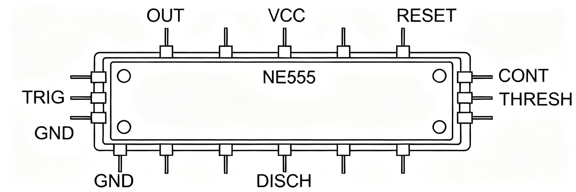
What the NE555 is and core building blocks
Point: The NE555 is a bipolar timer IC combining comparators, a flip-flop, a discharge transistor and an output stage to form a versatile timing block. Evidence: Internally, two comparators set thresholds at 1/3 and 2/3 VCC that drive the SR latch; the discharge transistor clamps the timing capacitor. Explanation: This architecture yields stable monostable, astable and gated modes with simple external R–C networks; for a basic description, treat the device as a compact timer IC building block in most low-frequency designs.
Typical applications and why it’s still used
Point: The NE555 is widely used for pulse generation, delays, LED flashers, tone generation, PWM and basic motor control. Evidence: Its appeal comes from simple component counts, timing from microseconds to hours with a single R–C network, and output drive capable of sourcing/sinking tens of milliamps. Explanation: Engineers and hobbyists pick the NE555 for quick proofs-of-concept, low-cost embedded timers and for robustness where MCU overhead is unnecessary; its forgiving wiring and clear formulas make it a go-to component.
2 — Key Technical Specifications
Electrical parameters to report (table-ready)
Point: Key parameters to list in a spec table include supply voltage, supply current, threshold/trigger levels, output high/low levels, source/sink current, timing range, maximum frequency, power dissipation and operating temperature. Evidence: Typical datasheet rows specify Symbol, Min/Typ/Max and test conditions (VCC, TA). Explanation: Capture min/typ/max where available and note test conditions so readers can interpret timing accuracy and thermal limits when selecting package and supply decoupling.
| Parameter | Symbol | Min | Typ | Max | Notes |
|---|---|---|---|---|---|
| Supply voltage | VCC | 4.5V | 5–9V | 15V | Recommended range; check datasheet |
| Supply current | ICC | — | 6–10mA | 15mA | Depends on output state |
| Trigger/Threshold | Vth/Vtr | 1/3·VCC | — | 2/3·VCC | Comparator references |
| Output source/sink | Iout | — | ~200mA | — | Peak currents; use buffering for inductive loads |
| Timing range | t | µs | ms–s | hours | Set by R and C; capacitor leakage matters |
| Operating temp | TA | -40°C | — | +85°C | Package dependent |
Recommended spec-table layout and callouts
Point: Use columns: Parameter | Symbol | Min | Typ | Max | Test conditions | Notes to keep data actionable. Evidence: Callouts should flag specs that drive design: output drive, supply limits and timing tolerance. Explanation: Add inline notes for measurement conditions (VCC, TA) and tooltips for designers—e.g., specify whether timing numbers assume ideal capacitors or include leakage; highlight when buffering is needed for sustained loads.
3 — Pinout & Functional Description
Pin-by-pin breakdown (pins 1–8)
Point: Each of the eight pins has a defined role; practical tips reduce common errors. Evidence & Explanation: See ordered list for canonical names and a one-line usage tip for each pin.
- GND — Ground reference; ensure low-impedance return and single-point tie to bypass cap.
- TRIG — Trigger input for monostable; short negative pulses below 1/3 VCC initiate a cycle.
- OUT — Output source/sink; can drive LEDs/relays briefly but buffer for continuous inductive loads.
- RESET — Active-low reset; tie high if unused, add pull-up to avoid spurious resets.
- CTRL — Control voltage; bypass with 0.01µF to ground or use to modulate duty via external voltage.
- THR — Threshold comparator input; monitors timing capacitor voltage to end a pulse.
- DISCH — Discharge transistor; connects timing capacitor to ground during discharge intervals.
- VCC — Positive supply; place bypass capacitor close to this pin.
Typical wiring patterns for monostable & astable modes
Point: Standard formulas let designers calculate R and C for target timing. Evidence: Monostable pulse width t = 1.1 × R × C (R between VCC and capacitor, C to ground). Astable frequency f = 1.44 / [(R1 + 2R2) × C], duty = (R1 + R2)/(R1 + 2R2). Explanation: Use low-leakage electrolytic or film capacitors for long intervals and respect polarity on electrolytics; decouple CTRL when seeking accurate timing.
4 — Key Performance Metrics & Design Considerations
Accuracy, stability and timing tolerance
Point: Timing error arises from resistor tolerance, capacitor tolerances and environmental factors. Evidence: A 5% resistor and 20% capacitor can yield ±25% timing variance; temperature coefficients of capacitors add drift. Explanation: Mitigate with 0.1%–1% resistors, C0G/NP0 or film capacitors, local temperature control and bypassing the control pin to reduce supply ripple influence.
Output drive, protection and power management
Point: The NE555 can source/sink moderate currents but has thermal and current limits—buffer when driving motors or coils. Evidence: Repeated high-current switching increases power dissipation; inductive loads need flyback diodes or external drivers. Explanation: Place a 0.1µF bypass at VCC-GND, keep traces short, and use series resistors or MOSFET drivers for sustained loads; use RESET to disable output safely during power-up.
5 — Practical Examples & Troubleshooting
Compact example circuits to include
Monostable delay example: R = 470kΩ, C = 10µF → t ≈ 1.1 × 470kΩ × 10µF ≈ 5.17s; expect tolerance from component specs. Astable LED flasher: R1 = 1kΩ, R2 = 100kΩ, C = 10µF → f ≈ 1.44 / [(1kΩ + 2 × 100kΩ) × 10µF] ≈ 0.72Hz; verify duty with scope. PWM via CTRL: apply a variable 0–VCC control on CTRL with bypass to vary threshold and modulate duty in real time.
Common failure modes and step-by-step debugging checklist
- Verify VCC and GND continuity and correct polarity; check bypass cap at VCC.
- Confirm RESET is held high; tie to VCC if unused.
- Check trigger wiring and capacitor polarity; replace suspect electrolytic caps.
- Probe at OUT and DISCH to isolate IC vs. external load; substitute a known-good IC if behavior persists.
- Escalate to buffered driver if output cannot source required current or shows thermal foldback.
Summary
The NE555 provides a predictable, low-component-count solution for timing needs when designers understand its specs, internal thresholds and pinout behavior; using proper decoupling, precision R–C choices and buffering for loads yields reliable timers. This brief offers the specs and pinout guidance needed to design, prototype and troubleshoot robust NE555-based circuits while balancing timing accuracy and output constraints.
- NE555 core value: simple timer IC functionality with easy R–C timing—select resistors and capacitors to control tolerance and stability around the provided specs.
- Pinout best practices: tie RESET high, bypass CTRL with 0.01µF, place VCC bypass close to the IC to minimize supply ripple affecting timing.
- Design trade-offs: use precision resistors and low-leakage capacitors for accuracy; buffer outputs for inductive or high-current loads to protect the NE555.
FAQ — NE555 Common Questions
How do I calculate NE555 monostable pulse width?
Use t = 1.1 × R × C where R is between VCC and the timing capacitor and C is from timing node to ground; account for resistor and capacitor tolerances and use low-leakage capacitors for long delays.
What is the NE555 pinout for control and reset?
Reset is active-low and should be tied high if unused; CTRL (control) is pin 5 and benefits from a 0.01µF bypass to ground to stabilize internal comparator thresholds and improve timing stability.
When should I buffer the NE555 output?
Buffer the output when driving sustained loads, inductive devices or when required current exceeds the device's safe operating limits; using drivers or MOSFET stages reduces IC heating and improves reliability.
How do I mitigate timing errors in high-precision NE555 applications?
Mitigate timing instability by using 1% or better precision resistors, stable C0G/NP0 or film capacitors instead of leaky electrolytics, placing a 0.1µF decoupling capacitor close to VCC/GND, and bypassing the CTRL pin to decouple supply noise.


