Despite modern microcontrollers, the 555 family remains a pervasive choice in both hobbyist and industrial schematics because of its simplicity, low cost, and predictable analog timing behavior. This article translates the NE555N datasheet into actionable specs, practical limits, and design rules so engineers can move from datasheet numbers to reliable circuits. Readers will get pin functions, core electrical limits, timing formulas, thermal and noise guidance, testing steps, and a quick-reference checklist.
The focus is practical: identify which datasheet numbers matter for layout and safety, how timing accuracy is affected by component choices, and how to test and troubleshoot a 555-based circuit on the bench. Key terms used here include NE555N, datasheet, and specs; where manufacturer values vary, ranges are shown and readers are advised to confirm the exact numbers for the part ordered.
NE555N Overview & Pin Functions
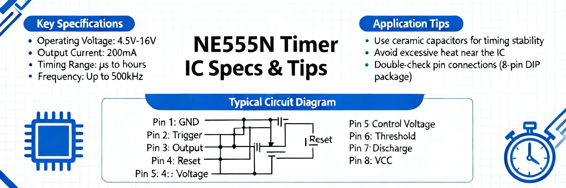
The NE555N is a bipolar-timer IC with eight pins arranged for common astable and monostable configurations. Designers rely on the internal comparators and flip-flop to translate voltages on threshold and trigger into timed outputs; the comparator thresholds are at approximately 1/3 VCC and 2/3 VCC, which underpin standard timing formulas. This paragraph states the behavioral point, the datasheet evidence (comparator thresholds), and why it matters: thresholds set the switching points for timing accuracy.
Pinout at a glance
Point: Each pin has a dedicated, repeatable role. Evidence: datasheet pin descriptions map functions to pins. Explanation: GND (pin 1) is circuit reference; VCC (pin 8) powers the chip; Output (pin 3) delivers the timed signal; Reset (pin 4) active-low clears the internal latch; Control (pin 5) accepts an external reference to alter thresholds; Threshold (pin 6) and Trigger (pin 2) are comparator inputs; Discharge (pin 7) is an open-collector transistor used to discharge timing capacitors. Knowing each pin prevents common wiring errors and aids fast bench debugging.
Package variants & nomenclature
Point: The “N” suffix typically indicates a plastic DIP package variant intended for through-hole use; alternatives include SOIC and other surface-mount variants. Evidence: datasheets list mechanical package options and thermal resistance values. Explanation: Use DIP for breadboarding and prototyping; choose SOIC for automated PCBs and tighter thermal constraints. Package choice affects thermal dissipation and PCB layout, so pick with assembly and thermal budget in mind.
Core Electrical Specifications
Point: Electrical limits determine what the IC can drive and how it behaves under stress. Evidence: typical datasheet fields include operating VCC range, absolute maximum, quiescent current (ICC), and output-drive capability. Explanation: translating those numbers into design rules prevents over-voltage, excessive heating, or unwanted loading of the output.
| Parameter | Minimum Range | Maximum Limit | Design Margin Recommendation |
|---|---|---|---|
| Supply Voltage (VCC) | 4.5 V | 16 V (Abs Max 18 V) | Keep within 5 V to 15 V operational range |
| Output Current (Source/Sink) | — | 200 mA (Abs Max) | Buffer continuous loads exceeding 50 mA |
| Quiescent Current (ICC) | 3 mA | 15 mA (at VCC = 15V) | Factor into thermal budget calculations |
| Discharge Pin Current | — | 50 mA | Protect with series resistor for high-capacitance discharge |
Supply & absolute limits
Point: Typical operating VCC ranges found in common NE555N datasheets are in the mid single-digits to mid-teens of volts; absolute maximum values sit higher but must not be exceeded. Evidence: manufacturer datasheets typically specify an operating range (for example, roughly 4.5–16 V) and an absolute maximum slightly above that. Explanation: stay well within the datasheet operating range in production; add margin in designs and include over-voltage protection or series resistance if supply transients are possible.
Output & discharge characteristics
Point: The output stage can source and sink notable instantaneous currents but has thermal and average-current limits. Evidence: datasheets specify source/sink capabilities and discharge-transistor ratings. Explanation: while the output may momentarily drive tens to a couple hundred milliamps, continuous loads above about 50 mA should be buffered. The discharge pin is designed to sink timing capacitor currents; large capacitors or inductive loads can overstress that transistor without a buffer.
Timing Behavior & Frequency Limits
Point: Timing depends on the internal comparator thresholds and the charge/discharge path of the timing capacitor. Evidence: the standard formulas derive directly from 1/3 and 2/3 VCC comparator thresholds and the internal discharge transistor behavior. Explanation: use the formulas but respect the device’s switching speed limits and component parasitics to avoid unexpected behavior at extremes.
Timing formulas & thresholds
Point: Use established equations for reliable design. Evidence: astable high time t_high = 0.693*(Ra+Rb)*C; low time t_low = 0.693*Rb*C; monostable t = 1.1*R*C; thresholds are at ~1/3 and ~2/3 VCC. Explanation: these closed-form relations let designers size R and C to target period and duty cycle; the 0.693 and 1.1 coefficients come from ln(2) and RC time-constant integration tied to comparator thresholds.
Practical frequency bounds & accuracy
Point: Practical timing range is wide, from milliseconds to hours, but not without limits. Evidence: switching times, discharge-current limits, and comparator response in datasheets constrain minimum periods; component leakage and temperature coefficients limit long-term accuracy. Explanation: avoid attempting periods below ~10 µs without characterization; above kHz ranges, waveform distortion and comparator propagation delay reduce accuracy. For long-period timing, use low-leakage capacitors and account for resistor temperature drift.
Thermal, Noise & Control-Voltage Considerations
Point: Thermal dissipation and noise coupling determine reliability and jitter. Evidence: datasheet thermal resistance and ICC figures allow dissipation estimates; control-pin behavior is explicitly documented. Explanation: combine measured ICC and VCC to estimate power dissipation, account for package thermal resistance, and design PCB layout and decoupling to keep junction temperature safe.
Power dissipation & thermal limits
Point: Estimate IC dissipation from supply current and switching behavior. Evidence: typical approach is PD ≈ VCC × ICC + switching losses; datasheet gives thermal resistance (θJA) for package. Explanation: compute junction temperature rise (PD × θJA) and ensure it stays below safe limits; derate supply or add buffering if the calculated junction temperature approaches thermal limits during continuous operation.
Control pin, decoupling, and layout tips
Point: The control pin modifies comparator thresholds; layout and bypassing reduce jitter. Evidence: datasheets recommend bypass caps on control and VCC pins. Explanation: place a 10 nF bypass from control to ground to stabilize thresholds, use a 0.1 µF VCC-to-GND bypass close to the IC, and keep timing capacitor traces short. These steps reduce false triggers and phase noise.
Practical Design Guidelines & Worked Examples
Point: Selecting resistor and capacitor values trades stability against size and leakage. Evidence: timing formulas plus capacitor datasheet leakage and ESR specs drive choices. Explanation: choose R values large enough to limit discharge currents but not so large that input bias and leakage dominate; pick C types with low leakage for long periods and low ESR for high-frequency stability.
Sizing R and C for target frequency/duty
Point: Worked example — design an astable near 1 kHz with ~55% duty. Evidence: using t_high = 0.693*(Ra+Rb)*C and t_low = 0.693*Rb*C, pick C = 0.01 µF, solve for Ra and Rb. Explanation: for f ≈1 kHz, T ≈1 ms; choose Rb ≈ 7.5 kΩ, Ra ≈ 6 kΩ to get ~0.55 duty. Use 1% resistors for improved accuracy and a CNP or film capacitor if stability is important.
Driving loads & buffering recommendations
Point: Buffer outputs when driving moderate or inductive loads. Evidence: output stage ratings and typical recommended continuous-current limits. Explanation: use a dedicated driver or a small MOSFET/BJT stage for loads above ~50 mA; add a flyback diode for inductive loads and a series resistor for LEDs to limit current and protect the chip.
Common Failure Modes & Test Procedures
Point: Failures often stem from decoupling, wrong component values, or thermal stress. Evidence: recurring fault patterns in bench troubleshooting align with datasheet cautions. Explanation: systematic isolation reduces debug time — check supply rails, reset, control pin, and timing capacitor first before swapping the IC.
Typical faults & root causes
Point: Frequent issues include stuck outputs, unstable timing, or heat-related drift. Evidence: root causes include missing bypass caps, wrong polarity electrolytics, or oversized timing capacitors. Explanation: verifying wiring, component orientation, and the presence of recommended bypass components resolves most faults quickly.
Bench tests & measurements
Point: Use a checklist of checks and oscilloscope probe points. Evidence: expected pin voltages in idle and oscillating states come from comparator thresholds and output states. Explanation: measure VCC, verify ~1/3 and ~2/3 VCC behavior at trigger/threshold during transitions, observe output waveforms at pin 3, and use a multimeter to confirm no short circuits or unexpected currents before dynamic testing.
Quick Reference Specs & Practical Checklist
One-page spec summary to include
- Operating VCC range (typical datasheet): choose a supply within the datasheet’s specified operating range; confirm absolute max before release. This protects the IC and sets timing reference points for threshold voltages and formulas.
- Comparator thresholds and timing formulas: 1/3 VCC and 2/3 VCC underpin t_high = 0.693(Ra+Rb)C, t_low = 0.693RbC; use these for all timing sizing and verification.
- Quiescent and output limits: use datasheet ICC to estimate PD = VCC×ICC; avoid continuous output currents above recommended continuous values—buffer outputs for >50 mA loads to prevent overheating.
Design do's & don'ts checklist
- Do bypass VCC within 1 cm of IC with 0.1 µF and provide 10 nF on control pin; reduces jitter and false triggers.
- Don't use extremely small C (<100 pF) without characterization; stray capacitance and comparator propagation will dominate at high frequencies.
- Do prefer film or NP electrolytic for long periods; ceramic MLCCs have higher dielectric absorption and can alter long timing.
Summary & Next Steps
Three takeaways: first, the comparator thresholds (≈1/3 and 2/3 VCC) and the standard timing formulas are the foundation for any NE555N timing design; second, obey electrical and thermal limits from the datasheet and buffer outputs when in doubt; third, layout and proper decoupling directly affect jitter and reliability. These points translate datasheet numbers into everyday design rules.
Next steps: apply the worked example to your BOM, run the quick-reference checklist on a prototype, and validate timing across temperature with real capacitors and resistors. Keep a printed one-page spec list with the critical datasheet numbers for on-bench reference and consult the specific NE555N datasheet for exact absolute-maximum values for your supplier’s part.
FAQ: NE555N common questions
Can the NE555N drive an LED directly?
Yes for brief pulses: the output can source/sink tens of milliamps, so a single LED with a series resistor is acceptable for short or low-duty applications. For continuous currents above ~50 mA, use a buffer transistor or dedicated driver to avoid stressing the IC and increasing dissipation.
How accurate are timing intervals from the datasheet formulas?
Accuracy depends on resistor tolerance, capacitor type, temperature drift, and control-pin stability. The formulas are accurate in theory, but expect percentage errors from component tolerances; use 1% resistors and low-leakage capacitors for higher accuracy and add temperature compensation if required.
What are the quickest bench checks to isolate a faulty 555 circuit?
Verify VCC and ground, ensure reset is held high, check for the presence of bypass capacitors, measure trigger/threshold voltages during transitions, and replace the timing capacitor with a known-good part. These steps often identify wiring or component faults before replacing the IC.


