The LM555 remains a fundamental timer IC for engineers designing oscillators and one‑shot circuits. This deep dive turns datasheet figures and RC formulas into a practical checklist, showing how pin behavior and electrical specs translate to predictable timing. It references standard timing equations and pin functions to shorten the path from spec sheet to working prototype.
Data-driven hook: the RC timing equations (t = 1.1 × R × C for monostable mode and f ≈ 1 / (0.693 × (RA + 2RB) × C) for astable mode) form the baseline for thousands of timing designs. Practical notes cite datasheet tables and test graphs to quantify tolerances and limits for robust circuits.
1 — Background: LM555 at a glance
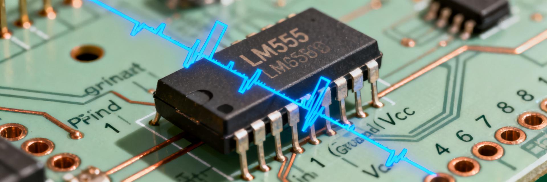
Device family and package overview
Point: The LM555 is offered in common 8‑pin DIP, SOIC and low‑power variants. Evidence: datasheet package tables list single timers and reduced‑power suffixes and recommended VCC ranges. Explanation: designers choose the package variant for supply range (typically single‑supply operation) and thermal considerations for intended applications like timers, PWM and simple oscillators.
Functional block summary
Point: Internally the LM555 uses two comparators, an SR flip‑flop, a discharge transistor and an output stage. Evidence: refer to the datasheet block diagram showing comparator thresholds tied to 1/3 and 2/3 VCC and the discharge transistor on the threshold pin. Explanation: map comparator thresholds to trigger/threshold pins to predict when the output toggles and how the discharge transistor clamps the timing node.
2 — Datasheet anatomy: key electrical specs & limits
Absolute maximums vs recommended operating conditions
Point: Absolute maximum ratings exceed recommended operating conditions and must not be used as design targets. Evidence: datasheet tables separate VCC maximum, input voltage limits and junction temperature from recommended supply ranges. Explanation: use recommended VCC margins and derating (e.g., a safe operating window several volts below absolute max) to avoid latent failures and ensure long‑term reliability.
Electrical characteristics that affect timing
Point: Timing depends on comparator thresholds (1/3 and 2/3 VCC), control pin behavior, supply current and output drive. Evidence: electrical characteristics and timing‑vs‑temperature graphs in the datasheet quantify tolerance and drift. Explanation: account for control‑voltage tolerance, supply variation and temp drift when calculating worst‑case timing and jitter for a given R and C.
| Specification Parameter | Typical Recommended Value | Absolute Maximum Limit | Design Impact on Timing |
|---|---|---|---|
| Supply Voltage (VCC) | 4.5V to 15V | 16V to 18V | Directly scales threshold window stability |
| Output Driver Source/Sink | Up to 200 mA | 225 mA | Determines rise/fall times & load capability |
| Timing Accuracy Temp Drift | 50 ppm/°C | N/A | Affects precision over standard ambient shifts |
3 — Pinout explained: role, voltages, and practical notes
Pins 1–4: Ground, trigger, output, reset
Point: Pins 1–4 handle ground, trigger input, output, and reset; each has expected DC behavior. Evidence: datasheet pin descriptions show trigger threshold near 1/3 VCC and active‑low reset behavior. Explanation: tie reset high if unused, keep trigger input filtered to avoid false trips, and expect the output to source/sink limited current per datasheet drive specs.
Pins 5–8: Control, threshold, discharge, VCC
Point: Control (CV) alters threshold reference, threshold pin senses the timing capacitor node, discharge provides fast discharge path, and VCC requires bypassing. Evidence: datasheet recommends 0.01 µF on CV and shows discharge transistor timing curves. Explanation: decouple VCC close to the IC and bypass CV to stabilize thresholds; short leads on control/trigger traces reduce noise sensitivity.
4 — RC timing analysis: monostable & astable derivations
Monostable timing: derivation, practical formula, and limits
Point: Monostable pulse width follows t = 1.1 × R × C under the datasheet assumptions. Evidence: derive from exponential charge to 2/3 VCC with threshold at 2/3 and trigger at 1/3; datasheet capacitor‑charge graphs validate. Explanation: include component tolerances, minimum resistor to protect discharge transistor (often ≥1 kΩ), and capacitor leakage when computing worst‑case pulse width.
Astable timing: frequency, duty cycle and stability
Point: Astable frequency approximates f ≈ 1 / (0.693 × (RA + 2RB) × C); duty = (RA + RB)/(RA + 2RB). Evidence: datasheet timing equations and graphs show frequency dependence on supply and control voltage. Explanation: compensate for control pin deviations and tolerance stacking (resistors ±%, C tolerance) when selecting RA, RB, C for target frequency and duty cycle.
5 — Practical design tips: component selection, PCB, and robustness
Choosing resistors and capacitors for accuracy & reliability
Point: Resistor minima, capacitor type and tolerance determine stability and lifetime. Evidence: datasheet cautions on excessive discharge current through low R; ESR and leakage affect timing. Explanation: use ≥1 kΩ for timing resistors in many ranges, choose film or C0G ceramics for precision in µs–ms ranges, and electrolytics only for long‑time constants where leakage is acceptable.
Layout, decoupling and noise mitigation for predictable timing
Point: PCB layout and decoupling significantly affect real‑world timing. Evidence: datasheet recommends decoupling close to VCC and CV pins. Explanation: keep trigger and CV traces short, use local ground returns, place 0.01 µF on CV and 0.1 µF on VCC adjacent to the package, and verify with proper scope probing to avoid added stray capacitance.
6 — Test, debug and validation checklist
Bench testing sequence and oscilloscope checks
Point: A systematic bench routine validates the design against datasheet expectations. Evidence: measure DC pin voltages first, then trigger/threshold waveforms and compare pulse width/frequency to calculated values. Explanation: use a 1×/10× probe appropriately compensated, place ground clip carefully to avoid ground loops, and log temperature to correlate timing drift with datasheet curves.
Common failure modes and fixes
Point: Symptoms like no oscillation or erratic timing have repeatable remedies. Evidence: common causes listed in troubleshooting guides mirror datasheet cautions (reset floating, leaky caps, noisy control pin). Explanation: try tying reset high, increasing resistor values to limit discharge stress, replacing suspect capacitors, and adding CV bypass or small input filtering to stabilize behavior.
Summary
- Use the LM555 datasheet to confirm absolute and recommended limits; design margins must be set below absolute maximums to ensure reliability and long life.
- Map the functional block diagram to the pinout to predict node behavior; control pin decoupling and short trigger traces are essential for stable timing.
- Apply t = 1.1×R×C and f ≈ 1/(0.693×(RA+2RB)×C) while stacking tolerances and considering ESR/leakage to compute worst‑case timing and jitter.
Frequently Asked Questions
What are the essential LM555 datasheet limits to check before design?
Check recommended VCC range, absolute maximum VCC, input voltage limits, junction temperature and output drive current. Verify timing versus temperature graphs and control‑voltage specs to define worst‑case margins. Document these values and include decoupling and derating in the design checklist.
How does the LM555 pinout affect timing and wiring?
Pin functions (trigger, threshold, discharge, control, reset) determine where noise and stray capacitance matter most. Keep trigger and CV wiring short, bypass CV, and provide solid ground return. Miswiring reset or leaving control floating are common causes of erratic timing.
How accurate are LM555 monostable timing calculations from the datasheet?
Nominal formulas give good first‑order results, but accuracy depends on resistor and capacitor tolerances, leakage, ESR, supply variation and temperature. Use tolerance stacking to compute min/max pulse widths and validate on the bench against datasheet timing‑vs‑temperature curves.
What is the minimum resistor value recommended for the LM555 discharge pin?
To protect the internal open-collector discharge transistor (Pin 7) from excessive current stress when the timing capacitor discharges, a series timing resistor (typically RA) of at least 1 kΩ is highly recommended. Values below this can degrade or permanently damage the transistor over active switching cycles.


