Across hobbyist and legacy power designs, the IRF510 MOSFET still appears in thousands of schematics because its datasheet lists a 100 V drain-to-source rating and chipset-style test figures that make it tempting for mid-voltage, low-frequency uses. Point: the raw ratings lure designers; Evidence: datasheet headline numbers such as VDS ≈ 100 V and ID ratings are prominent; Explanation: those numbers require interpretation before being treated as safe continuous limits in a real design.
Purpose: this article translates datasheet numbers into usable limits and trade-offs for US engineering practice.
Point: designers need concrete derating, thermal, and switching guidance;
Evidence: common mistakes are assuming test-condition RDS(on) equals real-world conduction resistance and ignoring SOA;
Explanation: the goal here is pragmatic, stepwise guidance to move from the published specs to a reliable implementation.
Quick background: What the IRF510 MOSFET is and where it shows up
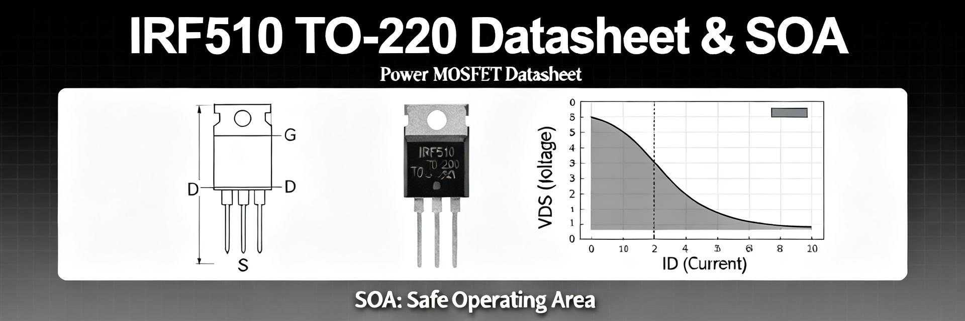
Technical family and typical package
Point: the device is an N-channel enhancement-mode power MOSFET in a through-hole TO-220 style package commonly used in audio, hobby power, and vintage designs.
Evidence: the part’s construction and package favor moderate power dissipation with optional heatsinking.
Explanation: that packaging and device family make it suitable for linear stages and low-frequency switching where thermal mass and heatsinks can control junction rise, not for high-frequency, high-efficiency converters.
Typical datasheet headline numbers
Point: datasheet raw ratings typically advertise VDS max ≈ 100 V, ID continuous around 5–6 A, and an RDS(on) on the order of 0.3–0.6 Ω.
Evidence: those numbers are test or maximum figures rather than guaranteed continuous operating points.
Explanation: designers must treat these as starting points, then apply derating for ambient temperature and SOA.
| Parameter Decoder | Datasheet Peak | Practical Design Limit |
|---|---|---|
| VDS (Drain-Source) | 100 V | 80 V - 90 V (Derated) |
| ID (Continuous) | ~5.6 A | Depends on Heatsink (often < 3A) |
| VGS (Gate-Source) | ±20 V | 10 V - 12 V for full Switch |
Key absolute ratings decoded (datasheet safe limits)
Voltage and current limits (VDS, VGS, ID)
Point: absolute ratings like VDS(max), VGS(max), and ID(max) define failure boundaries, not normal operating points.
Evidence: VDS(max) ~100 V is the avalanche limit; VGS(max) is typically ±20 V; ID(max) is often given as a pulsed or case-cooled value.
Explanation: you must derate—use a comfortable margin on VDS (10–20%), keep VGS within safe gate-drive limits, and use thermal derating to translate pulsed ID into reliable continuous current.
Thermal and SOA (Safe Operating Area) implications
Point: thermal resistance (RθJC / RθJA) and SOA curves control continuous dissipation.
Evidence: RθJA for a bare TO-220 can be tens of °C/W, making even a few watts raise junction temperature significantly; SOA curves show sharply reduced allowable VDS×ID at longer pulse widths.
Explanation: interpret datasheet SOA to avoid secondary breakdown—limit VDS and current during startup, inductive switching, or fault conditions, and design a thermal path to keep Tj below the device limit with margin.
Static and dynamic electrical specs: RDS(on), threshold, capacitances
Interpreting RDS(on) and ID-VDS curves
Point: RDS(on) is specified at a particular VGS and temperature and increases with junction temperature.
Evidence: datasheet RDS(on) may be stated at VGS=10 V and 25°C; ID–VDS curves show non-ideal, temperature-dependent behavior.
Explanation: compute conduction loss as I^2·R and include margin—designers should assume RDS(on) rises by tens of percent at elevated Tj.
Threshold, Transconductance, and Capacitances
Point: VGS(th) is a threshold for measurable conduction, not the gate drive needed for low RDS(on).
Evidence: threshold may be a few volts but full conduction often requires 8–12 V gate drive; total gate charge and Ciss determine driver current.
Explanation: use a driver sized for the gate charge, expect slow switching with large Ciss, and factor switching losses.
Switching behavior and practical limits for designers
Switching losses & Driver requirements: Point: switching energy depends on gate charge Qg and the overlap of voltage and current. Evidence: datasheet switching graphs show longer rise/fall at higher capacitances; Explanation: add a gate resistor to damp oscillations and accept that this device suits low-frequency switching.
Safe use cases vs. Avoidance: Point: IRF510 is poor for high-efficiency, high-frequency converters. Evidence: moderate RDS(on) and large capacitances create high losses. Explanation: prefer for audio amplifiers or simple regulators; choose modern MOSFETs for high-efficiency buck converters.
Real-world derating, thermal management and PCB tips
Heatsinking & Junction Temperature: Point: junction temperature follows Tj = Ta + Pd·RθJA. Evidence: without a heatsink a TO‑220 part can have RθJA in the tens of °C/W. Explanation: use PCB copper pours or a heatsink to reduce RθJA; aim for junction margin (e.g., 50°C below max).
Protection & Margining: Point: protecting against inductive spikes prevents failure. Evidence: snubbers reduce VDS overshoot; gate-stoppers limit spikes. Explanation: add RC snubbers for inductive loads and sense-based current limiting to protect the device.
Short worked example (numeric)
Target: 50 V, 2 A DC load check
Evidence & Explanation:
1. Assume RDS(on)=0.54 Ω @ 25°C
2. Conduction Pd = I^2·R = 4·0.54 = 2.16 W
3. If RDS(on) +50% at high Tj (≈0.81 Ω), Pd ≈ 3.24 W
4. To hold Tj rise < 50°C, RθJA must be ≈ 50°C / 3.24 W ≈ 15°C/W
Result: Requires heatsink or large PCB copper.
Key Summary
- Treat datasheet headline numbers as starting points: confirm VDS and current with margin and translate RDS(on) into real conduction loss.
- Account for dynamic specs: use the device’s gate charge and Ciss to size a driver; IRF510 performs best at low switching frequencies.
- Design thermal path first: compute Pd, select heatsink or copper area to meet a target RθJA, and add protection for transient conditions.
Common questions & answers
Can an IRF510 handle continuous 5 A current?
Point: datasheet ID ratings may list higher currents, but continuous current depends on thermal path. Evidence: a 5 A continuous current with moderate RDS(on) will produce several watts of heat; Explanation: unless RθJA is low, continuous 5 A will overheat the device.
What gate drive voltage does an IRF510 need for low RDS(on)?
Point: threshold voltage and test VGS differ. Evidence: VGS(th) is typically a few volts, but low RDS(on) requires higher gate drive. Explanation: to achieve near-spec RDS(on) you typically need a gate drive in the 8–12 V range.
Is the IRF510 suitable for switching at tens of kHz?
Point: switching suitability depends on capacitance and RDS(on). Evidence: large input capacitance and gate charge increase switching energy. Explanation: at tens of kHz switching losses become significant; use the IRF510 only for low-frequency or linear roles.
Technical Guide for IRF510 MOSFET Design & Specification Interpretation | Electronics Engineering Resource


